So a while back I saw this video on Youtube by "Gary Explains" talking about a "One Instruction Set Computer".
For those who do not know, a computer processor does a fixed set of things or follows a fixed set of instructions. Usually modern processors have hundreds of instructions.
In the OISC or URISC (Ultimate Reduced Instruction Set Computer) processor the idea is to have one universal instruction that the processor executes that allows the programmer to write any program.
The first time I heard of this idea I fell off my chair with excitement (Literally). My mind was really blown by the fact that you could write any program with just one instruction.
So after going through what "Gary" on Youtube had to offer... I sat down and tried to come up with a design of this hypothetical processor that executes only one instruction.
In the video Gary talked about a processor that executed an instruction called 'SUBLEQ' which simply means,
SUBtract and then branch if the result is Less than or EQual to zero.
While I dug the idea, I realized something....
to detect if the answer is negative or not we only need to look at the MSB (Most Significant Bit) of the result. But, to detect if the result was zero or not required an extra circuit, an 8 input NOR gate.
So, I thought why bother detecting the zero in the first place?? lets just do a branch if the answer is negative!!(turns out it wasn't really a break through.... a simple Wiki search shows up an instruction called 'SUBNEG' that does exactly that ...LOL.....)
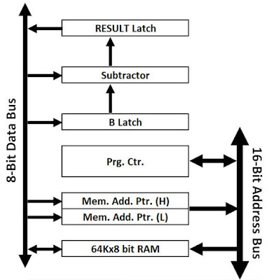
So, I sat down to come up with a simple design for my computer and this is the architecture I came up with:

The processor executes just one instruction consisting of a single arithmetic operation and conditional branching called 'SUBNEG' i.e. subtract and then branch if negative.
The instruction directly operates on the memory and requires 3 memory locations. The first 2 memory locations contain the data that needs to be operated on and the 3rd location is the branch/jump address.
So, suppose the 3 locations were B,A,C
the instruction executes in the following manner:
1) Take data in location B and subtract it from data in location A
2) Save the result in location A
3) If the result was a negative number jump to memory location C else continue to next memory location.
Each memory location or Address is 16-bits wide i.e. 2 bytes, hence the whole instruction takes 6 bytes of program memory.
The processor has two 16-bit registers namely:-
Program Counter and Memory Address Pointer,
and two 8-bit registers namely:-
B latch/register and Result latch/register.
Apart from this it has an 8 bit subtractor with one input coming from the Data Bus and the other from the B register.
In the next post I'll try explaining the control word and the micro-instructions decoding stuff.....till then....
Got any queries???E-Mail me at: shashwath.sundar@gmail.com
Comments
Post a Comment